| Service Hotline: | 0755-25566186 |
| 130-6691-6396 |
| Service Hotline: | 0755-25566186 |
| 130-6691-6396 |

Shenzhen Juke Industry Co., Ltd.
Tel: (86) 755-25566186
Fax: (86) 755-29668058
E-mail:jakizhu@163.com
Contact:
Zhu Wenwu
Mobile: 13928444330
QQ: 504060299
Zhu Ganghui
Mobile: 13714798680
QQ: 1046243838
Miss Zhou
Mobile: 13066916396
QQ: 1253838927
Address:1006 Huamei Building, Huamei Road, Songgang, Bao'an District. Shenzhen

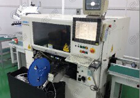
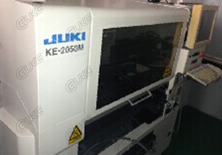
Product Name:JUKI KE2060 Mounter
Product Specifications: 1,400×1,393×1,440mm
JUKI Mounter KE2060
Board Size
M Board (330×250mm) For
L Board (410×360mm)
Lwide (510×360mm)
E Board (510×460mm)*1
Mountable Component Size:
Laser Recognition 0603 Chip ( Inch 0201) Chip ~33.5mm square element
image recognition 1.0×0.5mm*2 to 74mm square element
or 50×150mm (0402 (inch 01005) chip requires options) *9
element placement speed:
chip element 12,500CPH*3
IC element 1,850CPH*3*4
Component placement accuracy:
Laser recognition ±0.05mm
image recognition ±0.03mm (±0.04mm when using MNVC (optional))
Component placement type: 80 types (converted to 8mm belt) *6
Machine size: 1,400×1,393×1,440mm
Machine weight: About 1,410kg

Welcome to know/procure the JUKI KE2060 placement machine.

KE2060
machines can also be used for high-speed mounting of small components in addition to ICs or complex shaped heterogeneity components.
12,500CPH: chip (laser recognition / actual production ergonomics)
1,850CPH: IC (image recognition / actual production ergonomics),
3,400CPH: IC (Image Recognition/Using MNVC)
Laser Head × 1 (4 Nozzles) & High-Resolution Visual Head × 1 (1 Nozzle)
0603 Chip (Inch 0201) Chip ~ 33.5mm Square Element
0402 (01005 inch) chip at the factory option
image recognition (reflective / transmissive identification, ball identification, segmentation identification)
1 placement speed difference while 2 without more information, see the catalog

substrate size M substrate ( 330 × 250mm) L substrate (410 × 360mm) Lwide (510 × 360mm) E substrate (510 × 460mm) * 1
of the laser chip identification 0603 (0201 inch) square chips ~ 33.5mm element
image recognition 1.0 × 0.5mm * 2 ~ 74mm square element or 50 × 150mm 0402 (inch 01005) chip requires options) Component placement speed Chip component 12,500CPH*3, IC component 1,850CPH*3*4
        3,400CPH*5
Component placement accuracy Laser recognition ±0.05mm
image ±0.03mm (±0.04mm when MNVC (option) is used)
80 types of component placement (converted to 8mm tape) *6
*1 The mounter for E-size substrates is produced after order.
*2 When using a high-resolution camera (option).
*3 Actual work efficiency: The chip placement speed is the conversion value when 400 1608 components are mounted on the entire surface of an M-size board.
The mounting speed of IC components is the conversion value when 36 QFPs (100 pins or more) or BGA (256 balls or more) are mounted on an M-size substrate.
(CPH = average number of mounted components for 1 hour)
*4 Conversion value when feeding matrix trays.
*5 Conversion value when using MNVC (option) and full nozzle at the same time.
*6 Up to 110 varieties can be used with multi-layer pallet changer.